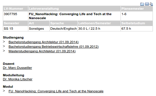
Difference between revisions of "NanoHacking-UNILI"
(→Group 2 - MAKE) |
(→Group 2 - MAKE: Manue) |
||
| Line 90: | Line 90: | ||
[[File:sample_2.jpg|400px]] | [[File:sample_2.jpg|400px]] | ||
| − | === [[Group 2 - MAKE: | + | === [[Group 2 - MAKE: Manuel]] === |
'''manuelW:''' | '''manuelW:''' | ||
Revision as of 16:34, 4 May 2015
"The innovators of 1600 were hackers before the word existed; they proposed open sharing of ideas for the benefit of humanity. Isaac Newton, Robert Hooke, Descartes, and the other scientists of the late 1600s could not have inaugurated the greatest scientific innovation of all time—the invention of modern science itself—without the Hackers of the 1600s. The Renaissance’s secretive structure was hacked, and it inspired the Scientific Revolution."
Contents
- 1 News
- 2 Where
- 3 Projects
- 3.1 Group 1 - SEE
- 3.2 Group 1 - MAKE - Claudio
- 3.3 Group 2 - SEE
- 3.4 Group 2 - MAKE: Manuel
- 3.5 Group 3 - SEE - Raphael, Kevin, Barbara, Janine
- 3.6 Group 3 - MAKE - Raphael, Kevin, Barbara, Janine
- 3.7 Group 4 - SEE- Anastasiia, Sevak, Christoph, Philip
- 3.8 Group 4 - MAKE - Anastasiia, Sevak, Christoph, Philip
- 3.9 Group 5 - MAKE - Barbara
- 4 Sandbox - NanoHacking UNILI
- 5 Schedule
- 6 Presentation-slides
- 7 Who
- 8 Description
- 9 Related
- 10 Furter readings and interesting links
- 11 Videos
News
- 23.April: RAUMÄNDERUNG: Ab 24. April finden sämtliche Veranstaltungen im Seminarraum 3 / S3 statt.
Where
http://www.uni.li/tabid/251/id/43034.67/default.aspx
Projects
Group 1 - SEE
Group: Steffi, Hassan, Omer, Stephan
Building a microscope
Step 1.
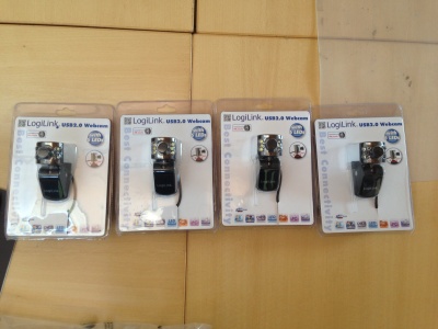
Install the webcam on the computer.
Step 2.
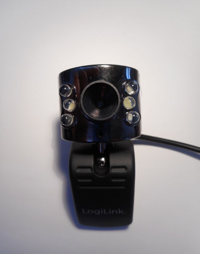
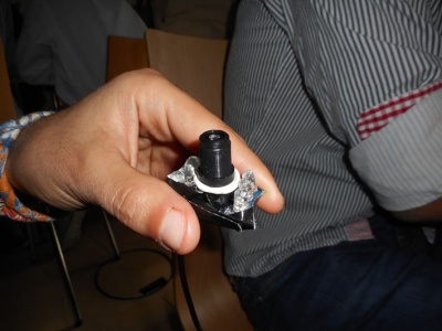
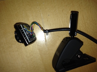
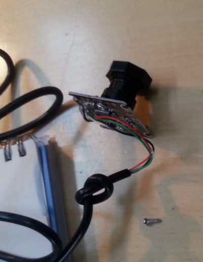
Take apart the webcam into it`s components until the image sensor and the electronics are disclosed.
(image will be uploaded)
Setp 3.
Turn the Lens (Objektiv) and stick it to the image-sensor to get a microscope.
Step 4.
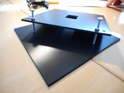
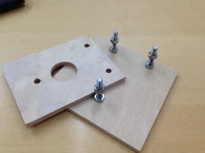
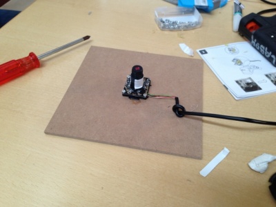
Build a stable case or a Box for the microscope (lens and the electronics).
Combine the Lens or the case with a mechanism for the distance-control for better adjustments afterwards.
Step 5.
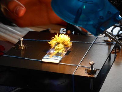
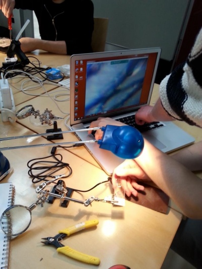
Put an object (flower, seeds, etc.) above the lens and adjust the lens until it can be seen in a good quality.
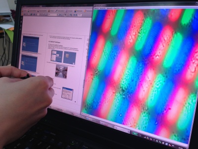
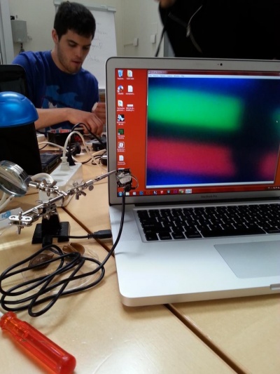
The camera sends the videodata from the Microscope to the laptop. The Object can be seen in nanoscale on the screen of the laptop.
Group 1 - MAKE - Claudio
Group 2 - SEE
Group Members: Sabrina, Manuela, Claudio, Manuel
Step 1:
Install the driver of the webcam on the laptop and try to adjust the lens.
Step 2:
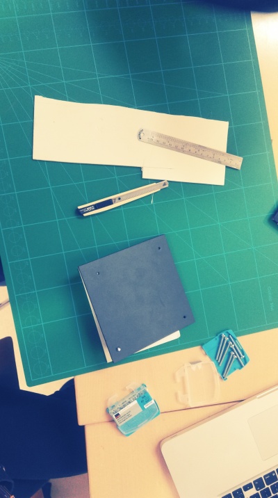
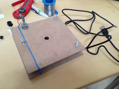
Split up the webcam into its electronic parts. Remove the case, edit the lens and flip it up site down. Build a stable construction/framework out of wood. Glue the “microscope” on the framework.
Step 3: Remove one LED from the webcam itself to extend the wires.
Step 4: Get a real-life sample/object out of the nature and make first attempts to adjust the lens.
Group 2 - MAKE: Manuel
manuelW:
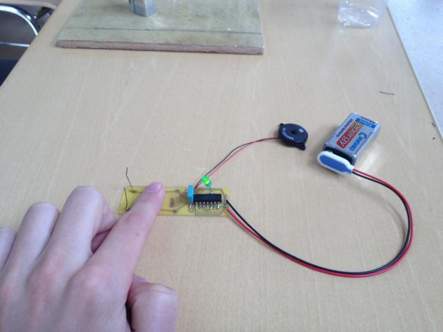
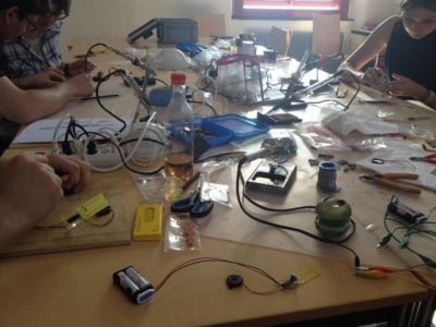
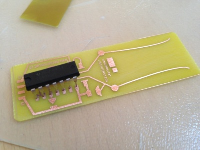
Today, the 25th April 2015 we build our own circuit board made out of conductive copper. For this we used templates to "draw" the circuit on the board with the help of a UV-light and acid
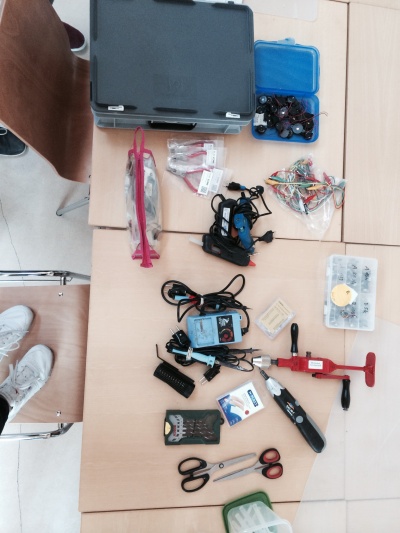
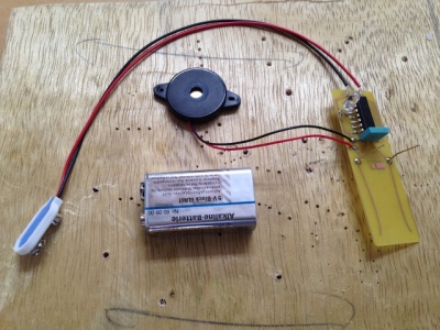
Used materials?: batteries with connection wire, wires (black and red),resistances, LED-lights, solder-iron, loudspeaker
Function?: by connecting the electric poles, we were able to hear a sound out of the speaker, depending on the resistance we used
Result?:
Group 3 - SEE - Raphael, Kevin, Barbara, Janine
Hacking a Webcam - The Process:
- Step: First we installed the software and the driver to use the camera as usual. This step does not really contain a hack :-)
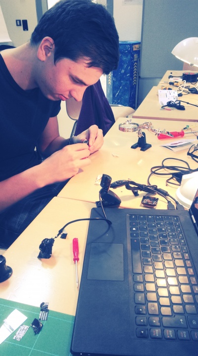
- Step: After that we removed the case to use and adjust the electronical parts as well as the lens to modify our microscope.
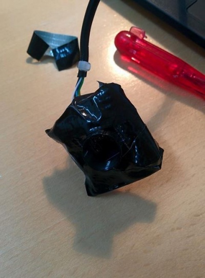
- Step: In the next step we changed the direction of the lens in order to hack its functions. Now the webcam serves as a microscope. We further cut of the LEDs and protected the circuit board from sunlight by using tape. In parallel we built a stable framework.
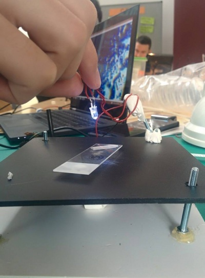
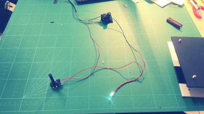
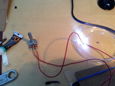
- Step: In the last step we added an LED and a potentiometer to adjust the brightness of the LED. Now we are to look at things on a very small scale.
Pictures of modification process:
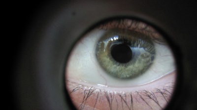
During the "Hacking a Webcam Process" we took pictures of our iris with the help of a mobile-cam + a additional lens
Outcome:
This is how our microscope looked at the end:
A resistor was used as a dimmer.
Resulting pictures:
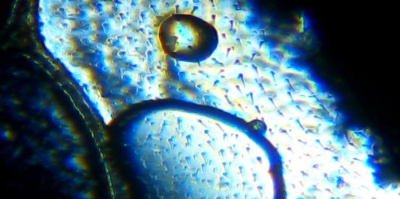
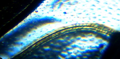
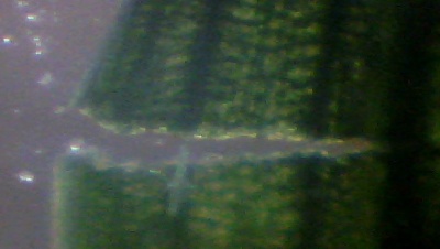
We analysed some kind of bug that we found outside. The images we produced "on a nanoscale" are showed in the following:
Group 3 - MAKE - Raphael, Kevin, Barbara, Janine
Kevin (keegan11):
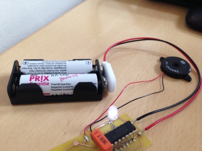
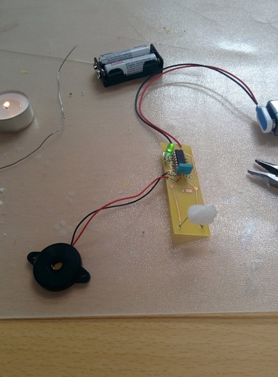
We made noise. Based on conductive copper, we used the sunglight, in more detail the UV light, to produce our circuit board. Accoringly we customized the basic circuit by just drawing things on the negative. After that we soldered the cuircit as illustrated in the image below.
Materials:
- batteries
- wires
- LEDs
- speaker
- circuit
- chip
- etc.
Function: When the poles are connected sound (some would say noise) is produced, depending on the resistence that ouccurs between the poles.
Result:
Raphael (Carapace):
The first project of the NanoHacking course was concerned with the modification of materials.
The preparation process:
1. In order to create a voice generating device we first used a template which we customized to give the board its individual layout.
2. Secondly we treated the board with UV light (Sunlight / UV device) to manipulate the first layer.
4. What is important to note is that in order to have a functioning circuit the board should not be too long in the sun.
5. Subsequently we treated the modified board with a chemical solution to bring our circuit to the surface.
The soldering process:
1. After the creation of the circuit we had to solder the essential components on the board. The following components were used in the process:
- prepared board
- chip
- batteries
- wires
- LEDs
- speaker
2. As a result of the soldering process we were able to create our own working device which is able to produce sound based on the resistance between the two poles at the back of the board.
Group 4 - SEE- Anastasiia, Sevak, Christoph, Philip
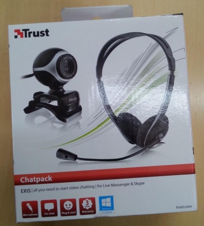
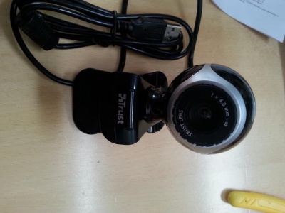
The process of building a microscope from a normal cam is the same as shown by other groups. The difference in the cam however bring some changes in the process. To show that every cam can be hacked and turned into a microscope our group choose a different cam version. We took two Trust cams and splited in two groups to work on different approaches. The main idea of the first approach by Anastasiia and Sevak (Sogomon) was to work on with the existing lens. The second approach done by Christoph and Philip worked with the integration of external lens on the Trust sensor.
The unboxing and dismantling of the cam is easy. Every cam has a way to open it since the cam was assembled with different parts from different manufacturers. This process took not more than 2 minutes.
The next step is to test the cam with an appropriate free cam software (since Trust does not deliver any own software). From here on the two approaches are not the same any more.
Approach One
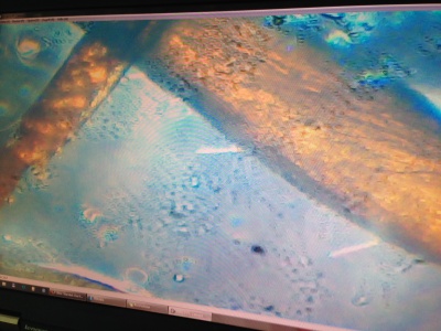
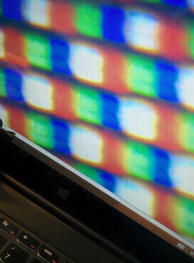
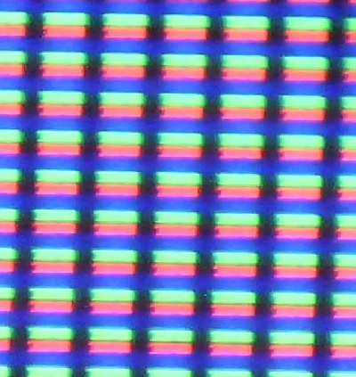
The following step after the dismantling is the manipulating of the lens. The lens of the cam has to be removed and reattached reverse on the sensor. The lens of the Trust cam revealed an unique property. The distance from the sensor to the lens is bigger compared to other cams (See Group 1-3). Since the distance is bigger we get more magnification. The result of higher magnification is shown in the next picture. We can observe here that the manipulated cam now can show one big pixel instead of many pixel (see sample pictures from other Groups).
However the big magnification brings also bigger problems with it. First the focus of the sample is bad. Second an adjustment with the hand is difficult since humans can not do small, precise movements without shaking. Finally it is more difficult to adjust the light to get clearer pictures. Nevertheless our first samples showed magnificent results.
As one solution to the problem we reduced the distance of the lens to the sensor by polishing the edges of the plastic-lens-holder and the plastic on the sensor. As expected the quality got better with less magnification. Also our Trust cam showed higher magnification as previous cams.
Approach Two
After the dismantling we added a external lens. We also reattached the lens reverse on the sensor.
The following step was to create a stable case or for the microscope. Now we were able to adjust the distance to the lens.
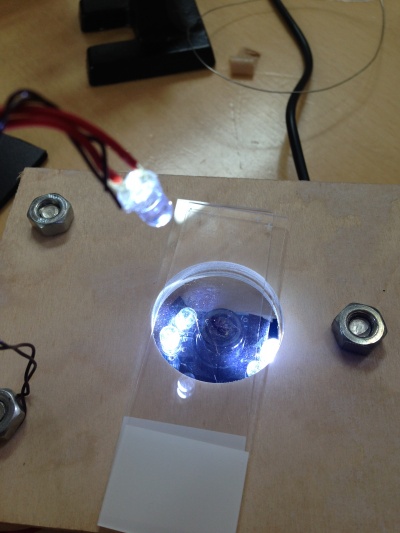
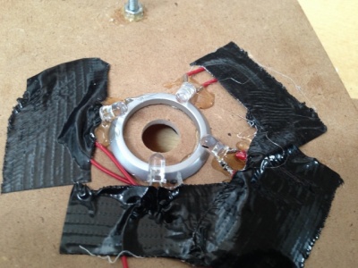
For a better picture we added four LEDs and a potentiometer to adjust the brightness of the LEDs.
Result:
Group 4 - MAKE - Anastasiia, Sevak, Christoph, Philip
From Sogomon, Pictures: christophobi
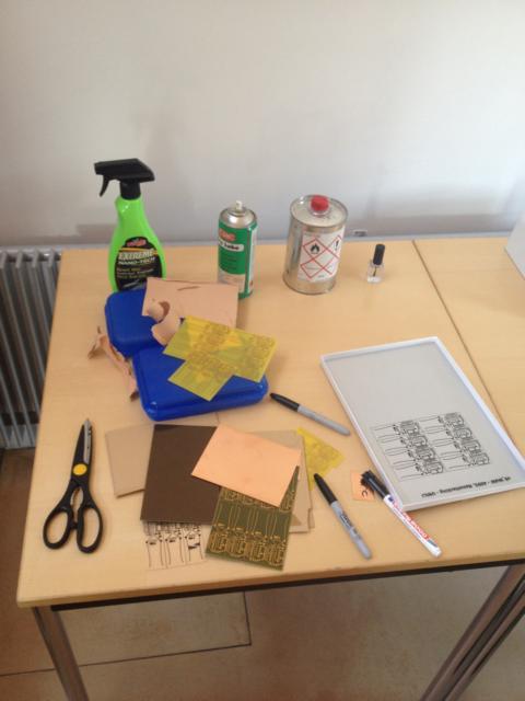
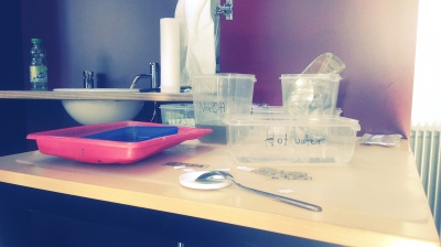
The making of a "nano"-sensor does not only include the assemble of different components, it is more. The very first step is to make one comfortable with the stuff one have. There are different materials with different properties and functions. One easy way to organize this different materials is to put them into groups or as we did to create special places such as the chemical lab and the making lab.
Next step on the way to the "nano"-sensor is to understand how things works. For example the process of creating a copper plate does not only requires copper but many other things. The theory explains that UV-light with the combination of chemicals can destroy copper layer on a plastic ground. The next steps show how it is done in more detail.
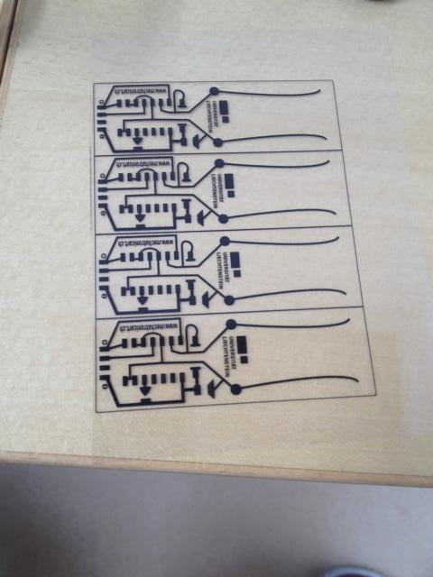
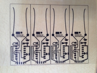
Step one: one has to choose the layout (in this case a circuit) which should remain a copper on a ground (this case plastic).
Here we can see the modification/resistance area of the layout. The future behavior of the sound can be manipulated here. However be careful not to connect the boarders of the resistance area.
Step two: the layout must be placed correctly (printed side on the top) on the copper and fix it with tape so the layout has no waves on the copper.
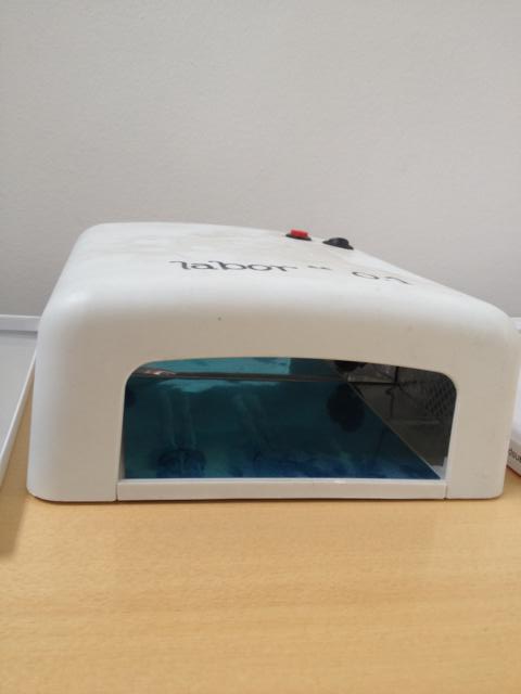
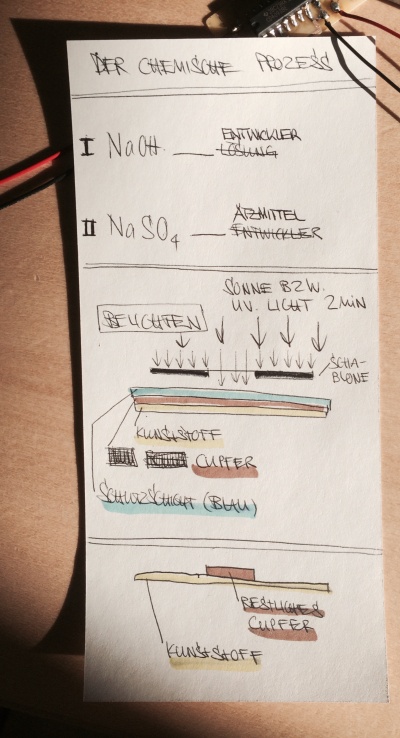
Step three: now the copper must be illuminated with UV light. This can be done with holding the copper under the sun for approx. 2 minutes or one can use UV-light-machine also maximum for 2 minutes illumination time. After the illumination the layout can be detached from the copperplate.
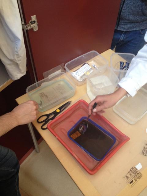
Step four: this step requires protective goggles since one has to work with chemicals. The copper plate now has to be bathed in a mix of water 1L and Sodium hydroxide (NaOH) 10g.
Step five: the next step is another bath for the copper. Now the copper plate has to be bathed in a mix of water 0.5L and Sodium persulfate (NaSo4) 100g. Here we have to wait until the illuminated part of the copper is etched away.
Now the copper circuit is done and ready to be used.
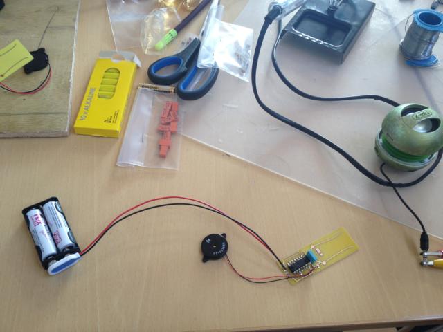
Step six: assembling the parts together. For this we need: wires, chip, battery, speaker, LED (optional). The next picture shows the place of components to be soldered. One must be careful here not to destroy the Plate and the connections on the plate.
Manipulation of the resistance area The resistance are can be coated with different materials and chemicals. For example lampblack, fire, dry lube and water show acoustic reactions. Other materials and chemicals such as extreme-nanotech-car-polisher, smartphone (music), wax showed no acoustic reactions at all. Here you are free to experiment and use whatever you think should/could/would show an acoustic resistance reaction.
Group 5 - MAKE - Barbara
Sandbox - NanoHacking UNILI
Schedule
Presentation-slides
Day 1 - Introduction
https://www.youtube.com/watch?v=UHCT9SOBHs0&feature=youtu.be
Day 2 & 3 - NanoHackLab
Setting up the Lab
Making Small Things
Dimensionality on the Nanoscale
Seeing Small Things
Surfaces and Interfaces
Day 4 - Group Works Start
Day 5 - Speculative Futures
Day 6 - Presentations
Who
Mentor - Dr. Marc Dusseiller (CH)
Dr. Marc R. Dusseiller is a transdisciplinary scholar, lecturer for micro- and nanotechnology, cultural facilitator and artist. He works in an integral way to combine science, art and education. He performs DIY (do-it-yourself) workshops in lo-fi electronics and synthesizers, hardware hacking, phyisical computing, nanotech and microscopy. He was co-organizing Dock18, Room for Mediacultures, diy* festival (Zürich, Switzerland), KIBLIX 2011 (Maribor, Slovenia), workshops for artists, schools and children as the former president (2008-12) of the Swiss Mechatronic Art Society, SGMK. In collaboration with Kapelica Gallery, he has started the BioTehna Lab in Ljubljana (2012 – 2013), an open platform for interdisciplinary and artistic research on life sciences. Currently, he is developing means to perform bio- and nanotechnology research and dissemination (Hackteria | Open Source Biological Art) in a DIY fashion in kitchens, ateliers and in developing countries.
Special Guest - Aurelio Lucchesi (CH)
Special Guest - Dipl.Ing. Urs Gaudenz (CH)
Students
- jayjay
- Omer.K
- hghayesh
- manuelW
- coconut91
- StephanOe (changed from Stephan)
- SabrinaU (changed from Sabrina)
- christophobi
- carapace
- keegan11
- BonsaiBob
- ueli
- babsiru
- oksivk
- doc1993
- sogomon
Description
Overview
During this course, the students will be introduced into the merging disciplines of of art, science and engineering that meet at the nanoscale. But what is nanotechnology? It promises huge beneficial impact on global health, sustainable energy and novel materials. At the same time utopian visions, science-fiction scenarios and fundamental fears are clashing at discussions in society. Throughout the course, we will lift the fogs of these superficial discussions and through hands-on activities get closer to grasp the world of the small. We will build our own simple DIY (do-it-yourself) optical and electronic instruments to learn more about nanoparticles and nanosensors, how to "see" them, how to "hear" them.
One key aspect of the nanosciences is the fact that the traditional disciplinary borders of physics, biology, engineering, to name a few, are merging. With the current tools and methods of understanding matter on the smallest scales of atoms and molecules, only a true collaborative and transdiscplinary approach can lead to new insight, application and constructive discourse of its societal implications.
more about project work and speculativ design thinking
Content (Englisch)
- Introduction to the science and technologies at the nanometer scale
- Overview of future technology trends involving nanotechnology
- Hacking as a method of creative thinking and opening the black box
- Practical laboratory experience in nanotechnology
- Societal implication of future technologies
- Methods for speculative design thinking
Lerninhalt (Deutsch)
- Einführung in die Wissenschaft und Technologien auf der Nanometerskala
- Überblick von zukunftsweisenden Technologietrends im Bereich der Nanotech
- "Hacking" als Methode kreativ zu Denken und die „Black-Box“ zu Öffnen
- Praktische Laborexperimente im Bereich Nanotechnologie
- Gesellschaftlicher Einfluss von Zukunftstechnologien
- Methoden für spekulatives „Design Thinking“
- Einführung in die Wissenschaft und Technologien auf der Nanometerskala
Related
Similar course done in Aalto University for High-School and Art Students NanoHacking: Converging Life and Tech at the Nanoscale - BiofiliA HighSchool, Finland
Furter readings and interesting links
NanoSmano
NanoŠmano - LifeSystems is an intersting art/sci collaborative research project, which happened 3 times in Ljubljana, Slovenia.
The following minimal circuit was developed as a DIY nano-based resistive surface sensor, introducing photolithography and surface properties, see Vive-la-Resistance
wetPONG
A course for bachelor students in biomedical engineering by the mentor, Marc Dusseiller, introducing a game-concept into the practical teaching of micro- and nanotechnology.
UCLA Sci|Art Nanolab
A 2 week summer-school for high-school students held every year at UCLA, combining artists and scientists as mentors.
http://summer.artscicenter.com/
Next Nature - Nanosupermarket
Critical Design & Speculative Futures
http://www.cd-cf.org/symposium/
http://www.extrapolationfactory.com/
https://squareup.com/market/the-extrapolation-factory
Articles
- "THE ART OF FREE AND OPEN SCIENCE", MCD#68 THE OPEN FUTURE see more info here and available for download in English and French
Videos
